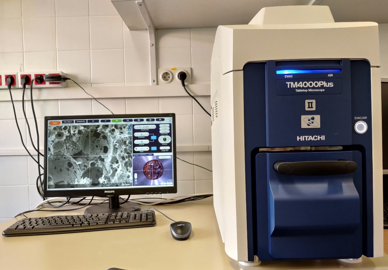
The U12 of NANBIOSIS (Nanostructured liquid characterization unit) has expanded its capabilities with a new equipment U12-E22. SEM Hitachi TM4000Plus II for morphological and dimensional characterization of solid samples
Low vacuum Scanning Electron Microscopy with two electron detectors (secondary, SE, and backscattered, BSE). SE imaging provides a detailed information of the morphology of the sample and BSE gives information about the different components of the sample, based on the different atomic number (the higher the atomic number, the brighter the surface).
The equipment can apply different vacuum levels (using a turbo molecular pump) with accelerating voltages between 5 and 20 kV and magnifications from 10x to 100,000x. Specimens with size up to 80 mm diameter and/or 50 mm thickness can be characterized and samples.
Conductive and non-conductive samples can be characterized with little or no previous preparation. The software enables image processing of micrographs, for instance, measuring the size of solid particles after the acquisition of images.
SEM analysis is very useful in several fields:
- Life sciences, for the topographical and morphological characterization of tissues, hairs, fibers, etc.
- Materials science, for quality control and failure analysis. Morphological properties are quite important in the research of innovative materials. In addition, the characterization of the surface is a key factor in porous materials used for delivery systems.
- Semiconductor inspection and microchip assembly, to analyse the topography and to investigate the effectiveness of production methods.
The equipment has been financed by CSIC and with funds of the research group coordinanting the unit from CIBER-BBN and IQAC-CSIC, led by Carlos Rodriguez-Abreu


